


What are the limitations of traditional electronic chips, such as GPUs, in handling the increasing demands of AI computing?
Traditional electronic chips, particularly GPUs, are facing several limitations in keeping pace with the explosive growth of AI. Firstly, Moore's Law, which predicted a doubling of transistors on a chip every 18-24 months, is slowing down, making it increasingly difficult and expensive to boost performance solely by shrinking transistor size. Secondly, large AI models consume vast amounts of energy, raising concerns about energy efficiency. Thirdly, a significant bottleneck exists in the transfer of data between the processor and memory, hindering overall computational speed. These factors collectively suggest that a new paradigm in computing is needed to overcome these limitations.
How does photonic computing differ from traditional electronic computing, and what are its potential advantages for AI?
Photonic computing uses light particles (photons) to transmit and process information, unlike electronic computing which relies on electrons flowing through copper wires. The fundamental advantage of photonic computing lies in the nature of light: it travels at a much higher speed and possesses a much larger bandwidth than electrons. In integrated photonics, optical components like lasers, modulators, and detectors are miniaturized onto a chip. Silicon photonics, a prominent approach, leverages the mature and cost-effective CMOS manufacturing processes of the semiconductor industry. By using light, photonic computing can potentially achieve significantly lower latency (delay) and reduced power consumption, making it highly attractive for AI applications that require processing massive datasets and performing complex matrix operations rapidly.
What is the core principle behind using photonic circuits to accelerate matrix operations, which are crucial for AI?
The core principle behind photonic acceleration of matrix operations lies in utilizing the wave properties of light, specifically interference and superposition. Photonic circuits, often based on architectures like Mach-Zehnder Interferometer (MZI) arrays or Wavelength Division Multiplexing (WDM), can perform matrix multiplications and accumulations "in-flight" as light signals propagate through the chip. By controlling the properties of light (e.g., intensity, phase) using components like modulators and phase shifters, the weights of a matrix can be encoded onto the light paths. As light beams interact within the photonic circuit, the resulting output directly corresponds to the result of the matrix operation. This inherent parallelism allows for simultaneous computations across the entire matrix, potentially achieving much higher speeds and lower latencies compared to the sequential processing in traditional electronic processors.
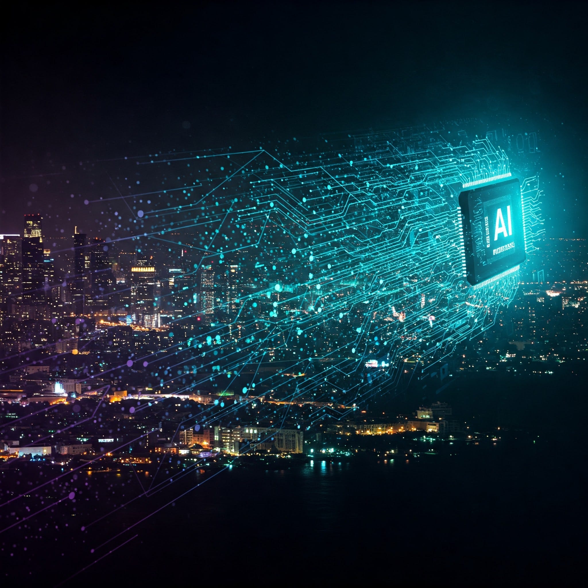
What is the PACE photonic accelerator, and what are its key features and demonstrated capabilities?
The PACE (Photonic Arithmetic Computing Engine) accelerator, likely developed by Lightelligence and detailed in a Nature paper, is a large-scale integrated photonic chip designed for ultra-low latency computation. Key features include the integration of over 16,000 optical components to create a 64x64 matrix processor. Its primary function is to perform linear matrix multiply-accumulate (MAC) operations and, notably, achieve very low operational latency of around 3 nanoseconds per cycle at a 1 GHz operating frequency. PACE employs a co-integrated electronic chip (ASIC) for logic, memory, and control, utilizing an innovative 2.5D hybrid advanced packaging technology for seamless integration. The accelerator has been demonstrated to be particularly effective in solving computationally intensive Ising problems, where its ultra-low latency provides a significant advantage.
Why is the problem of packaging so critical and challenging for the widespread adoption of photonic integrated circuits?
Packaging is a critical and often expensive challenge in the commercialization of photonic integrated circuits (PICs). Unlike electronic chip packaging, photonic packaging involves aligning tiny optical waveguides with other optical components (like fibers and lasers) with sub-micron precision, making it a time-consuming and costly process. The lack of standardization, the need for specialized materials and complex assembly techniques (like hybrid bonding), and the challenges of thermal management (given the heat generated by co-integrated electronic components) all contribute to high costs, potentially up to 80% of the total module cost. Overcoming these packaging challenges through innovations like advanced 2.5D/3D hybrid packaging, wafer-level/panel-level packaging, and automated passive alignment is crucial for achieving the scalability and cost-effectiveness required for widespread adoption of photonic computing.
What is the Ising problem, and why is the ultra-low latency of photonic accelerators like PACE particularly beneficial for solving it?
The Ising problem is a computational challenge rooted in statistical physics, which involves finding the lowest energy state of a system of interacting "spins." It serves as a mathematical model for many NP-hard combinatorial optimization problems found in diverse fields like finance, logistics, and materials science. Finding the exact solution to large-scale Ising problems is computationally very demanding for traditional computers. Photonic accelerators like PACE, with their ultra-low operational latency (e.g., 3 nanoseconds per cycle), are particularly beneficial for solving Ising problems because many heuristic algorithms used to find approximate solutions involve iterative processes. Each iteration's speed, heavily influenced by latency, directly impacts the overall time to find a good solution, especially for dynamic problems where the problem parameters change rapidly. The low latency of photonic cores enables faster iterations, potentially leading to quicker convergence to optimal or near-optimal solutions.
Beyond photonic accelerators for specific tasks, what other potential applications does silicon photonics have in the future of computing and technology?
Beyond accelerating specific computations like matrix operations and solving Ising problems, silicon photonics holds significant promise for various other applications. One key area is optical interconnects, where silicon photonics can provide high-bandwidth, low-power data transmission links within data centers and even between chips, overcoming the limitations of traditional copper interconnects. Other potential applications include biosensing (for highly sensitive medical diagnostics and environmental monitoring), LiDAR (for autonomous vehicles and robotics), and quantum computing (as a platform for manipulating and connecting qubits). The dual potential of silicon photonics for both computation and high-speed communication makes it a particularly compelling technology for future high-performance computing architectures.
What are the major hurdles that still need to be overcome for photonic computing to move from research labs to widespread commercial applications?
Several significant hurdles remain before photonic computing can achieve widespread commercial adoption. These include improving manufacturing yields and process maturity to ensure consistent performance at scale, drastically reducing costs, particularly in packaging and testing, establishing industry-wide standards for design, verification, and components, achieving reliable and cost-effective large-scale packaging and integration (including laser integration), enhancing the precision and stability of photonic analog computations for demanding applications, and developing a comprehensive software ecosystem and a skilled workforce capable of designing and utilizing photonic hardware. Overcoming these challenges requires continued innovation, investment, and collaboration across the entire photonics industry, from design tool developers to manufacturing facilities and end-users.
前言:AI 運算之牆與一道曙光
人工智慧(AI)的爆炸性成長,從 ChatGPT 到各種大型語言模型(LLM),正以前所未有的速度改變世界,但這背後是對運算能力近乎貪婪的需求 1。科技愛好者們可能已經感受到,傳統的電子晶片,特別是圖形處理器(GPU),似乎正撞上一堵無形的牆。摩爾定律(Moore's Law)的步伐明顯放緩 4,意味著單純依靠縮小電晶體尺寸來提升效能變得越來越困難且昂貴。同時,大型 AI 模型的驚人耗電量引發了對能源效率的擔憂 1,而處理器與記憶體之間的數據傳輸瓶頸也日益凸顯 3。這一切都預示著,我們需要一場運算領域的革命。
就在這個關鍵時刻,積體光子學(Integrated Photonics)帶來了一線希望。這不僅僅是微小的改進,而是一種潛在的典範轉移,承諾以光速進行運算,並可能帶來更高的能源效率 1。最近,像曦智科技(Lightelligence)和 Lightmatter 這樣的公司,正將這些充滿未來感的處理器從實驗室推向現實,引起了業界的廣泛關注 1。
光子運算的概念已經醞釀了數十年,但直到最近,技術的成熟度才足以讓我們看到實際的曙光。正如《自然》期刊的評論所指出的,這些最新的展示可能意味著我們終於能夠駕馭光的力量,來建構更強大、更節能的運算系統 5。特別是在 AI 對能源需求急劇增加的今天,這項技術的出現恰逢其時。這不僅僅是學術上的好奇,更是為了解決 AI 指數級算力需求與傳統電子元件物理極限之間的矛盾所帶來的迫切市場拉力。當 GPU 越來越熱、越來越耗電,產業界自然會積極尋找替代方案,而光子學正成為最有希望的候選者之一。
然而,我們也需要理解,光子學並非要立即全面取代電子學。至少在可預見的未來,它更像是一位強力的輔助者,專注於解決電子系統中最棘手的瓶頸,例如高速數據傳輸和核心的矩陣運算 1。目前的光子晶片仍然需要與電子晶片緊密協同工作,由後者負責邏輯、記憶體和控制等功能 1。因此,近期的發展重點將是混合光電系統,例如光子加速器或共封裝光學元件(Co-Packaged Optics, CPO),目標是提升整體系統在處理特定 AI 工作負載時的效能。
點亮未來:用光束進行運算
想像一下,電子在銅線中流動,就像汽車在擁擠的高速公路上行駛,時常遇到堵塞和延遲;而光子在光波導中穿梭,則如同子彈列車在專用軌道上飛馳,暢通無阻。這就是光子運算的基本魅力:利用光的物理特性來處理資訊。
積體光子學的核心思想,是將傳統光學實驗室中龐大的元件,如雷射、調變器、探測器和光波導等,微縮到一個小小的晶片上 7。而矽光子學(Silicon Photonics, SiPh)則是其中最受矚目的技術路徑,它選擇使用矽這種半導體產業最熟悉的材料來製造光子晶片 11。
這背後有一個非常務實的考量:矽光子學可以最大程度地利用數十年來為電子晶片產業投入數十億美元所建立的成熟、低成本的互補式金屬氧化物半導體(CMOS)製造流程和龐大產能 1。儘管矽本身並非完美的光學材料——例如,它的間接能隙特性使得它無法有效地發光,需要額外整合雷射光源 11;而且光在矽波導中傳輸也會有損耗 18——但藉助現有半導體基礎設施所帶來的巨大經濟和規模化優勢,使得產業界願意投入大量資源去克服這些挑戰,例如開發混合整合技術來加入雷射 18,或使用氮化矽等其他材料來輔助 11。可以說,矽光子學的成功不僅僅是物理學的勝利,更是製造經濟學的體現。
在矽光子晶片上,光子就像電子在電路中一樣,遵循著預設的路徑。這些路徑被稱為「光波導」(Waveguides),它們利用矽(折射率約 3.5)與周圍包覆材料(通常是二氧化矽,折射率約 1.5)之間的高折射率差,將光束縛在其中,實現類似光纖的「全內反射」原理,引導光線傳播 6。為了將數據「寫入」光束,需要使用「調變器」(Modulators),它們可以改變光的強度、相位或偏振狀態來編碼資訊 6。最後,當運算完成後,需要「探測器」(Detectors)將光訊號轉換回電訊號,以便電子系統讀取結果 6。此外,還有耦合器(用於分光或合光)、濾波器、交換器等元件,共同構成複雜的光子積體電路(Photonic Integrated Circuits, PICs)6。
矽光子學的優勢顯而易見:利用光的超高速度和巨大頻寬來傳輸和處理資訊 4,潛在地降低延遲和功耗 6。這使得它不僅在傳統的光通訊領域(如數據中心內部的高速連接)大放異彩 1,更為 AI 運算這類需要處理海量數據的應用,開啟了全新的可能性 7。
AI 為何偏愛光:矩陣運算的極速引擎
為什麼光子運算對 AI 如此重要?答案的核心在於「矩陣運算」。想像一個大型的深度神經網路,它由無數個相互連接的神經元組成。當數據流經這個網路時,每一層神經元都會對輸入數據進行加權處理,這個過程在數學上就是大量的矩陣乘法(Matrix Multiplication)或更具體的矩陣向量乘法(Matrix-Vector Multiplication, MVM)以及乘積累加(Multiply-Accumulate, MAC)運算 2。事實上,這些矩陣運算佔據了 AI 模型訓練和推理過程中最主要的運算負載,是名副其實的效能瓶頸 2。
傳統的電子處理器(如 CPU 或 GPU)在執行這些運算時,需要不斷地從記憶體中讀取數據,在運算單元中進行計算,再將結果寫回記憶體,這個過程既耗時又耗能。而光子電路提供了一種截然不同的解決方案。
利用光的干涉和疊加原理,光子電路可以在光訊號傳播的過程中「順便」完成矩陣運算。常見的架構包括馬赫-曾德爾干涉儀(Mach-Zehnder Interferometer, MZI)陣列 12 或基於波分複用(Wavelength Division Multiplexing, WDM)的設計 21。
以 MZI 陣列為例,一個 MZI 通常由兩個 50:50 的光耦合器(或多模干涉儀 MMI)和兩個臂組成,其中至少一個臂上裝有移相器(Phase Shifter)12。通過精確控制移相器(通常是利用熱光效應或電光效應改變材料折射率),可以改變光通過 MZI 後在兩個輸出端口的強度和相位分佈。將大量的 MZI 單元排列成網格狀(Mesh),就可以構成一個可程式化的光學處理單元。輸入光向量的每個元素被調變到不同的光路上,當光通過 MZI 陣列時,通過設定每個 MZI 的移相值(代表矩陣的權重),光束會發生一系列的干涉和疊加,最終在輸出端探測到的光強度(或相位)就直接對應著矩陣乘法的結果 1。
這種運算方式的核心優勢在於其內在的「並行性」。矩陣中的所有乘法和加法運算幾乎是同時完成的,因為它們就發生在光傳播通過晶片的物理過程中。這使得光子加速器有望實現遠超電子元件的運算速度和極低的延遲 1。Lightmatter 公司在 2020 年就曾展示其光子晶片在 MAC 運算上比頂級 GPU 快 10 倍,能耗降低 90% 8;麻省理工學院(MIT)的研究人員也在 2023 年推出了光子運算開發套件,將代表性深度學習模型的推理時間縮短了 300 倍以上(相較於 Nvidia A100 GPU)8。這些成果都印證了光子運算在加速 AI 核心運算上的巨大潛力。
不過,這種基於光強度或相位等連續物理量進行的「類比運算」,也帶來了挑戰。類比系統天生對雜訊和元件的微小偏差(如製造誤差、溫度變化)非常敏感 1。要達到數位浮點運算那樣的高精度,需要付出額外的努力 1。例如,Lightmatter 就採用了將電子晶片堆疊在光子晶片之上的 3D 整合方式,利用電子電路進行精確的數據控制和誤差校正,並開發了自適應區塊浮點(Adaptive Block Floating-Point, ABFP)等技術來提高運算精度 1。因此,光子加速器的實用化,很大程度上取決於能否通過巧妙的電路設計、校準技術以及光電混合控制,來有效管理這些類比運算的固有局限性。
此外,僅僅加速矩陣乘法本身是不夠的。AI 應用,尤其是模型訓練,需要能夠靈活調整權重 8。MZI 陣列等光子電路的可程式化和可重構性 12 就顯得至關重要。通過調整 MZI 中的移相器,可以改變光路徑的權重,讓同一塊硬體能夠執行不同的矩陣運算,或者實現神經網路的不同層級。這種靈活性是從固定功能的加速器邁向更通用的光子 AI 處理器的關鍵 1。


Share this post